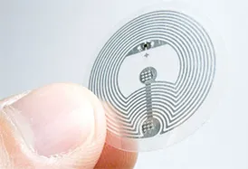
 Securing our increasingly connected world underpins its ability to enhance convenience and keep us all connected. With an ever-increasing number of smart devices communicating with one another, developers must protect each interaction from potential vulnerabilities. Near-field communication — NFC — technology helps safeguard the Internet of Things, with NFC readers providing a reliable layer of protection.
In part one of our NFC series, we identified many innovative ways to combat counterfeiting or gray market products and enhance the customer experience using NFC technology. With its short-range or localized communication providing product-specific information on or about consumable products like bottles or cartridges, NFC readers build a bridge between different connectivity protocols, enabling effortless device pairing and data exchange.
Now, we’ll dive into our thoughts on defining design requirements before getting into the good stuff in the third part of this series: picking the right NFC chip and tips and tricks for successfully implementing an NFC reader. Some concepts may have you dusting off old brain cells and digging into old engineering books, but application notes for most devices are pretty good, and the availability of low-cost and extremely useful test gear have made things so much easier.
Contents
NFC Building Blocks
NFC Reader and Tag Interaction
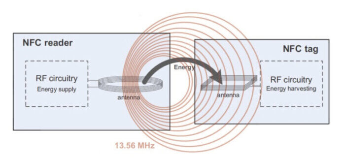
Source: STMicroelectronics
As mentioned in part one, NFC is based on inductive coupling. Think of it as an air-gap transformer. In a typical reader application, the “tag” is powered by harvesting the energy generated by the reader’s magnetic field. The transmitter drives an external antenna that generates the RF field and the transmitted carrier’s on-off keying (OOK) or AM modulation. Since the transmitter is the element responsible for generating the electromagnetic field, it can modulate the carrier directly. (i.e., direct modulation). Depending on the reader chip’s features, it may also support modulating externally.
The receiver “tag” detects this modulation superimposed on the 13.56 megahertz carrier signal and performs limiting and gain adjustments, filtering and demodulation to recover the data frames. When the tag responds, the outgoing data frames go back to the receiver. The process is very similar, with one slight difference using load modulation and one or two subcarrier frequencies.
 Which came first, the tag or receiver?
Both! There really is no wrong answer. When I work with clients, it always falls back to requirements and capabilities, with most relating to what is on the tag:
- Read distance.
- Size constraints of the product.
- Memory needs.
- Security features.
Tags in NFC Readers
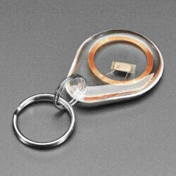 Key fob, wrist strap, card, puck, sticker, epoxy, embedded, big, small, square, round, visible, hidden … and the list goes on. There is a tag that is bound to work for you and many integrators (e.g., Tagify, HID, Identiv, Seritag) willing to help. A tag is basically the NFC semiconductor and antenna combined in a desired package or footprint.
Product offerings from semiconductor manufacturers are plentiful (e.g., STMicroelectronics, NXP), include powerful features and comply with International Organization for Standardization (ISO) and International Electrotechnical Commission (IEC) standards, such as 15693, 14443A, 14443B, FeliCa, NFCIP and others. As one would expect, different standards mostly define modulation type, data coding and the protocol used. The size of receiver and tag antennas is crucial when considering read distance and power consumption. The larger the antenna, the larger the magnetic field area and the greater the ability to couple at greater distances.
When selecting a tag, think about the following:
- Interface type (e.g., ISO/IEC15693)
- Distance and range
- Enclosure material — in a metal can, free space or other
- Storage capacity
- Data retention
- Endurance (write cycles)
- Segmentation of memory
- Password features
- Failed attempts counting
- Tamper detection
- Kill modes (deactivation)
- Temperature range
- Wet or dry
- Shock and vibration
 As an official ST Authorized Partner and ST Micro Partner Program member, we have often used the STMicroelectronics ST25TV series Type5 tag (ISO15693). Along with the ST25R3916B + antenna, tags can easily range to 10 cm. ISO15693 has a lower bandwidth, which makes achieving greater distances easier.
NFC Reader Receivers
The basic components of the receiver subsystem include the NFC chip/integrated circuit, EMI filter, antenna matching circuit and the loop antenna. This is the same circuit found on the STEVAL-ST25R3916B evaluation board, which is capable of all the operating modes (reader/writer, card emulation and active/passive peer-to-peer), complies with most standards — including ISO15693 — and uses slightly higher power for reading at greater distances.
Regardless of the NFC IC, the matching network elements will be fairly standard. NFC IC chip manufacturers often have matching tools that take much of the guesswork out of the design. Additional features found on the 3916B are AAT DACs (automatic antenna-tuning digital-to-analog converters) outputs that feed varicaps to adjust the serial and parallel matching using the IC’s internal registers as feedback to application firmware, which then adjusts between 0-3V.
This is a nice feature but has little practical value for the NFC circuit, as will be discussed later. However, it could come in handy for other design needs. I prefer a differential over a single-ended antenna interface due to the circuit’s better performance and EMI/EMC compliance testing.
Typical NFC Circuit
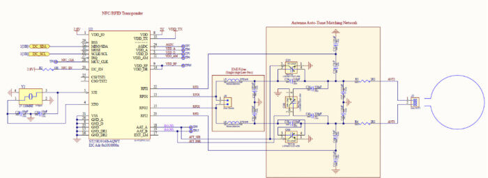
This is a single-stage low-pass filter made up of series inductors and parallel capacitors to ground aimed at suppressing harmonics.
This part of the circuit matches the impedance of the EMI filter and NFC IC to the antenna. The two series resistors used for quality factor — Q-factor — adjustment also affect the match. Varicaps provide a mechanism to tune on the fly but add little value, given a correct Q-factor. If space permits, one can always lay out the board with the varicaps, using them for engineering and prototyping but not populating for production. As neat as having varicaps in the design is, they have drawbacks — like the package being hard for contract manufacturers to assemble onto the board and very few manufacturers of the semiconductor itself.
Radiofrequency, or RF, “In” feeds the NFC IC receiver. The two caps work like a voltage divider. Typically not far from default evaluation board values, the matching tool helps ensure enough signal at the receiver for a good reading but not so much as to cause distortion.
These are used to adjust the Q-factor. When we think about RF, we want a very high Q-factor, but it can hurt us in NFC if too large. Tags are all different shapes and sizes, which affect the resonant frequency. Lowering the “Q” widens the bandwidth.
This is probably the hardest part. Understanding the expectations for the NFC IC is important, not just when designing your antenna coil but also when evaluating commercially available ones. In the case of the ST25R3916B, the sweet spot for series inductance of the antenna coil is 1-2 millihenries, whereas an NXP part might like a much higher series inductance. The goal is for the NFC IC to efficiently drive and generate the best electromagnetic field possible. More time will be spent characterizing and matching the antenna than almost anything else in your design.
Pro Tips
- If your antenna loop is integrated in the PCB and does not have a connector, add a header.
- Place a header between the EMC filter and the NFC IC.
- A header pitch of 2 mm or 0.100 inches works well to connect a vector network analyzer (VNA).
- Don’t forget test points.
Equipped with background knowledge about the critical components of NFC technology — from the role of tags to the intricacies of how receivers handle data — you can begin to move beyond the basics and explore how to pick the perfect NFC reader for your IoT design.
From Theory to Practice: What’s Coming in Part Three
Knowing how the pieces work is just the beginning. In part three of this blog series, we’ll explore advanced test tools like NanoVNA, show how to accurately measure tags, and uncover the secrets to optimizing your antenna for peak performance. Whether you’re designing a new connected device from scratch or enhancing an existing system, our next steps seamlessly bring everything together.
Looking to build smarter, more secure IoT systems? Let us know how we can help you refine your approach!
Check out part three in our NFC blog series: Building NFC Readers: Choosing the Right Chip and Implementation Tips.
