Now that we’ve detailed how near-field communication (NFC) readers help combat the threat of counterfeiting and gray market products and covered the basics of NFC readers — introducing the building blocks, tags and receivers — let’s move into selecting the right NFC reader, dive deeper into practical tools and measurements and see an example NFC reader in action.
Now that we’ve established the basics, it’s time to get strategic. Not all NFC readers are created equal — choosing the right one for your connected solution requires a precise balance between functionality, security and efficiency. Let’s dive into the decision-making process for selecting the ideal NFC chip, covering the critical factors that should shape your choice and some pro tips for seamless integration into your design to maximize performance and minimize headaches down the road.
Contents
NFC Readers: Making the Perfect Match
Each NFC chip has slightly different matching characteristics. In the case of the ST25R3916B and others, helpful information and tools guide you through tuning the matching network from application notes (ST: AN5276). The matching tool, combined with measurements taken with NanoVNA, often results in component values so close that fine-tuning may not be necessary.
Other than the “cool factor” and completely nerding out on coworkers, what is a vector network analyzer, or VNA?
A vector network analyzer characterizes the performance of RF and microwave components and systems by measuring magnitude and phase at multiple frequencies simultaneously. Collected data is then used to calculate the network’s impedance and the isolation and coupling between ports. Measurements include insertion loss, return loss and S-parameters of RF and microwave devices and systems, such as our matching network and antenna.
Inside the Vector Network Analyzer (VNA)

A measure of how much transmitted energy or power reflects from a discontinuity in a transmission line, the higher the return loss, the better the line performance.
NanoVNA
Do you have fond memories of Smith charts but not the budget for a big fancy network analyzer? You, my friend, are in luck! Allow me to introduce a piece of test gear you absolutely want on your bench — and not just for NFC matching: NanoVNA.
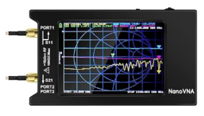 NanoVNA is a low-cost yet high-performance handheld VNA, with an LCD and a USB-C port for charging the 3.7V Li-ion battery and interfacing with a computer. A plethora of them are available at online retailers.
 NanoVNA is well known within amateur “ham” radio and hobbyist communities and has become the most popular VNA and antenna analyzer project since its early-2000s release.
The menu system will take a bit to get used to, or you may just jump straight to connecting via the USB-C to the application software to configure and drive the tool. The USB connection is generally the best option, providing better display readout and results capture for inclusion into engineering documentation.
Connecting the NanoVNA to your NFC matching network and antenna requires some thought. Due to space limitations, calibration standards are typically SMA and not as well suited for your actual design.
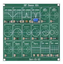
 A great addition to your NanoVNA is an RF demo card, which helps familiarize and teaches you how to use the VNA — and serves as a good sanity check for measurement setup. These cards come with some SMA-to-U.FL adapter cables and have the needed calibration terminations! This makes U.FL one good option for your design, but U.FL connectors are limited in the number of insertions and may wear out easily.
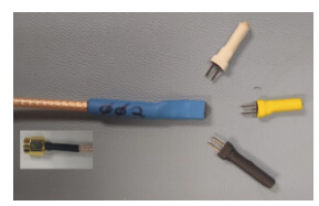
Alternatively, using 2-mm/0.1-inch headers between the NFC IC and matching network and antenna work well. SMA-to-header cables are easily made by modifying pre-assembled SMA cables. Calibration terminations use the mating header, surface mount resistors and different heat shrink colors for easy identification of the termination type (Open/50Ω/Short).
Calibration should be performed whenever the frequency range to be measured or interface cable changes. The calibration process compensates the NanoVNA and cables, so the actual measurement is the target circuit.
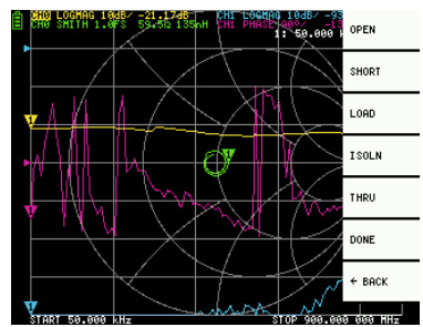 Set the START and STOP range from 10KHz to 100KHz.
- Reset the current calibration state.
- Connect OPEN standard to port1(CH0) and calibrate.
- Connect SHORT standard to port1(CH0) and calibrate.
- Connect the 50 ohm LOAD standard to the port1(CH0) and calibrate.
- THRU and ISOLN are typically calibrated, but we can skip this for NFC matching. Measurements for the matching network will only use port1(CH0).
Measuring the NFC Tag
One of the first experiments that’s fun to do with the VNA is measuring the resonant frequency of tags. The VNA is set up to read the logarithmic magnitude of reflected energy or “Log Mag.” Any basic loop of wire/antenna or even your antenna design connected to the S11 port of the VNA should expect to see a dip at around 13.56 MHz. It is not uncommon to see a tag has a higher resonant frequency. Remember, the tag antenna/coil will couple with the reader’s antenna and cause the frequency to shift downward. Proximity to metal, such as the enclosure, also has an effect. This can also be useful for a rough order of magnitude of how well the tag and reader couple.
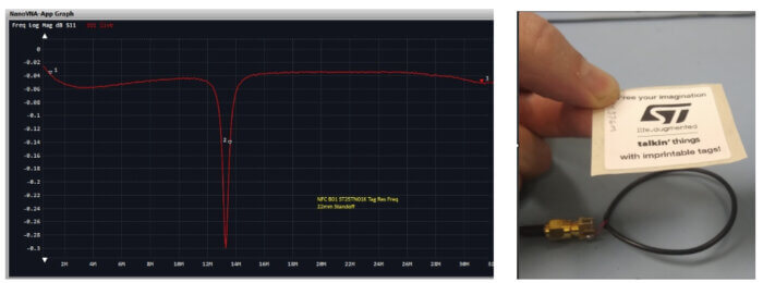
The VNA sweeps the signal source while reading the reflected energy. When a tag is present, due to the coupling, that energy transfers to the tag and is not reflected back, so this is why the dip or null is seen at the frequency of resonance.
Note: The loop antenna specifications are not critical. This two-inch loop diameter coil antenna was made from an SMA connector and six turns of magnet wire in a piece of heat-shrink tube.
Recall that credit cards also contain NFC tags and that this demonstration technique can gain access to your manager’s procurement card. Sadly, my manager saw it coming.
The NFC Antenna
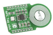 Fundamentally, the NFC antenna is a coil that will generate a magnetic field that powers and carries the modulated data when communicating with the tag. There are many “off-the-shelf” NFC antennas available from numerous manufacturers and in many different materials and form factors, but designing and integrating an antenna into the circuit board is not difficult.
Designing your own antenna gives the flexibility of accommodating mechanical form factors or cohabitating other features of the device (e.g., keyboard, capacitive touch). One does not have to look far online to find antenna design tools and calculators. Keep in mind that any metal or circuitry placed close to the NFC antenna (e.g., batteries, enclosure, other circuit boards, etc.) is likely to have a detuning effect on the antenna and affect performance. Creating isolation and shielding by adding a ferrite material to the antenna or enclosure may be necessary. Ferrite sheet may also be useful when taming those eddy currents generated in metal parts for EMI/EMC-related issues or creating isolation between other antennas. An excellent application note, AN11564 (NXP), describes this in greater detail.
Every antenna is composed of inductance (LANT), series (RS) and parallel (RP) resistances, and capacitance (CANT). These values and the self-resonance frequency determine the antenna equivalent circuit and Q-factor used to determine the matching network components.
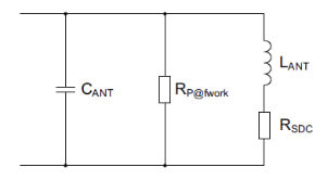 NFC IC datasheets and application notes will define recommended ranges for:
- LANT : Inductance of the antenna/coil
- CP(ANT) : Parallel or parasitic capacitance
- RS : Series resistance
- FSR : Frequency of self-resonance of the antenna/coil
There is somewhat of a chicken-and-egg problem between the NFC IC and antenna. Whether you decide to integrate your own or use an off-the-shelf option, antenna selection is such that one must be compatible with the other to achieve the proper performance (e.g.: An off-the-shelf antenna having an L, R and C higher or lower than those recommended by the NFC IC).
We recommend selecting the NFC IC first and leveraging the evaluation board and design for that vendor. Evaluation boards are great tools for validating read distance and other design requirements and as starting points for custom antenna designs. These boards also provide integrated software and tools that can be made to interface not just with your hardware but also for firmware development and more in-depth testing.
So, you’ve decided to design your own antenna. Antenna size, number of tracks, trace width/gap/thickness, inductance, series and parallel resistance, self-resonance frequency, and the Q-factor are all factors that determine the antenna’s electrical parameters. Because the antenna’s Q-factor can only be decreased (by damping resistors), the antenna must be designed with a Q-factor higher than the target system’s. The self-resonant frequency of the antenna should always be at least 25 MHz or higher.
Pro Tips
- Use the software app to control and view NanoVNA. As I found with the NanoVNA-App, configuration settings were easier to access and, in many cases, better than the device offered (e.g., higher number of points >400).
- Leverage evaluation board loop antenna designs.
- Design your own antenna — the availability and low cost of prototype circuit boards make evaluating the performance of different antenna designs and configurations easy.
- There is a tradeoff between the area/size of the coils and the inductance/series resistance. An NFC IC may not be able to pump enough drive current into the coil to achieve the desired read distance.
The antenna parameter measurements are gathered from the Smith chart (R + jX) display. Start with a frequency range or span set from 1 MHz to 300 MHz and measurement mode to S11 reflection measurement. Adjust the upper STOP frequency lower after identifying the self-resonant frequency of the antenna. After completing the calibration procedure with VNA and interface cable on the S11 port, connect directly to the antenna ends or connector. Disconnect the antenna from the reader and matching network. Take measurements as they would be in the device, as they would be with batteries and so on.
Note: Always ensure the NFC IC is not powered, which may damage the VNA!!!
In this example, the NanoVNA-App and markers positioned at 1 MHz, 13.56 MHz and real axis of the Smith chart (78.5 MHz) were used. Stop frequency of the span or impedance curve was lowered to 90 MHz or just beyond marker 3.
- Marker 1: 1 MHz values for series inductance and DC resistance:
- LANT = 2.110uH (For ST25R3916B 1.5-2.0uH is ideal)
- RS = 500mΩ
- Marker 3: Real axis where XL and XC cancel and values for parallel resistance and self-resonant frequency are taken:
- RP(FRES) = 7.032KΩ
- FRES = 74.536 MHz
Then, enter these values into the ST25R Antenna Matching Tool to calculate matching network component values.
Antenna and Matching Network
Some of the biggest factors influencing the NFC design performance are environmental conditions. As previously discussed, antenna loop diameter, reader-to-tag distance, enclosure material and other factors all come together and must be properly impedance matched to the NFC IC driver stage. The matching network plays an integral part in compensating for environmental factors, limiting unwanted emissions and determining power consumption. A mismatch can cause signal distortion, overshoot and EMI/EMC issues.
The EMI filter is simply a low-pass filter to filter out the higher harmonics created by the fast switching or edges. The cutoff frequency should be between 8 and 17 MHz. Generally speaking, the matching tools will produce a result using a 270nH chip inductor and adjust C (~680pF) to achieve the desired cutoff frequency. So yes, we know some of this is crazy talk, as the carrier is 13.56 MHz, so why even think less than 14 MHz? A cutoff frequency close to the carrier frequency will greatly decrease Q, so avoid a frequency between 13 and 14 MHz. As a starting point, roll with what the antenna matching tool suggests for values.
The capacitive voltage divider is all about the NFC IC and receiver path input level. We normally do not think of capacitors working in this way, but they do. As the designer, you will want to ensure enough signal going into the receiver port of the NFC IC, but not too much. Again, the matching tool typically provides the answer to the needed values.
The matching network follows the EMC filter with a primary goal of matching the antenna for maximum power transfer or current consumption target. We are also using the network to decrease the Q-factor of the antenna and convert it into the target Q-factor with the damping resistors. This conversion widens the reader bandwidth, accommodating the various resonant frequencies of the tags and so on. This is also why you may or may not want variable capacitors in the matching network, whether voltage-controlled or the classic trim capacitors. A valid case for inclusion could be a multi-NFC reader (e.g., more than two antenna coils) and physical layout different enough to affect the antenna match. The drawback is that somewhere in the manufacturing and test processes, someone will have to adjust it.
Our NFC Reader Example
So, let’s get some starting component values for the matching network calculated using our example antenna from earlier.
Antenna Matching Tool
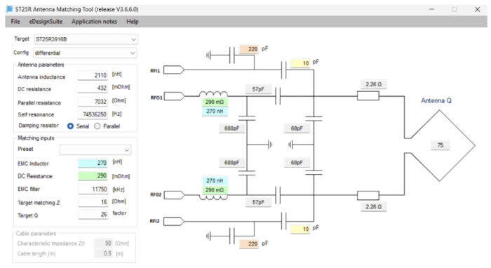
This is the ST25R antenna matching tool/software GUI, with the antenna parameters measured using the NanoVNA. I chose starting values for the EMC filter on the evaluation board, going with a target Q of 26 because the location and type of tag used was a “known quantity” and could reach the target distance with the least power required based on the antenna coupling (i.e., the diameter of the coils).
Now, enter the Smith chart. Recall what a Smith chart is all about: a graphical representation of the normalized impedance plotted in two dimensions. Resistance along the X-Y “real” axis, inductive “L” reactance above and capacitive reactance below. As is most often the case, measurements are normalized to 50Ω. It may take some digging, but each NFC IC will typically have an application note or two that shows a Smith chart and recommended sweet spot to target your match.
Examples shown are ST25R3916 left and NXP PN512.
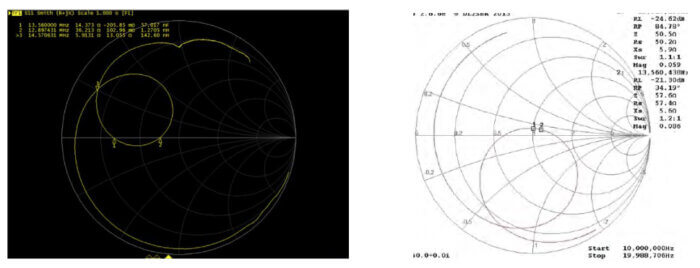
The goal is for the antenna match to be that of the expected driver impedance at 13.56 MHz. Now that we know what we are looking for, it’s time to connect up to our design, preferably in the final design configuration, and dial it in. This is done by connecting the VNA between the NFC IC and matching network and placing a header at that location. Always make certain the NFC IC is not active or driving the output! Set the VNA to S11 Smith (R+ jX), frequency span 1-30 MHz, and your markers.
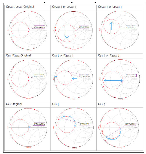
The second most valuable piece of information is a chart I snagged out of ST AN5276 Fig 27, which shows the cause and effect of resulting component value changes in the matching network. Armed with a small collection of component values, the match is easily dialed in.
Cause and Effect of Component Value Changes
Pro Tips
I built my product prototypes with the voltage-controlled varicap’s with the intent of dynamic match control. While informative and interesting, there is not much choice in the value range of these devices. Having gone with 100-200pF tune range, it was still above CS. The next lowest range was 30-60pF, which might have been more useful but was not available at the time of manufacture. Just be aware that if you are doing part number copy-pasta, change of value may be necessary.
Elevate Your IoT Design With NFCs
Creating your own NFC reader design and antenna and properly matching them remains difficult without the right knowledge — and can make or break your project. Application notes from the various NFC IC vendors are detailed, and excellent tools exist to design successfully. Armed with these resources and insights, you can make informed decisions that will elevate your IoT design to the next level.
But why stop here? Our team of IoT experts is ready to help you tackle the finer details, whether you’re looking for personalized guidance or want to discuss how NFC readers can fit into your specific application. Contact us today to start building the NFC-powered IoT solution your business needs.
