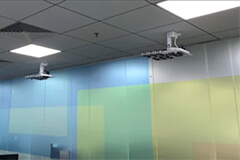
![]() With a dedicated Silicon Labs development center in Vietnam, we offer engineering services from the largest SiLabs team in the world (other than Silicon Labs itself). Established in 2019, the design center includes more than 100 employees supporting Silicon Labs directly, as well as delivering product development services to clients. A unique feature of the center is that we maintain a 150-node mesh network for extensive testing of device connectivity at scale.
With a dedicated Silicon Labs development center in Vietnam, we offer engineering services from the largest SiLabs team in the world (other than Silicon Labs itself). Established in 2019, the design center includes more than 100 employees supporting Silicon Labs directly, as well as delivering product development services to clients. A unique feature of the center is that we maintain a 150-node mesh network for extensive testing of device connectivity at scale.
Our familiarity with Silicon Labs’ 1) products, 2) development tools, and 3) manufacturing/commissioning processes, along with our extensive test bed, means we are the fastest way to get reliable connected products to market.
Our Dedicated Silicon Labs Design Services
Serving as Silicon Labs’ largest offshore partner, we offer global product design services for both their products and end-customers. Below are some of the common types of products we help develop, maintain and support.
Multi-Protocol Hubs
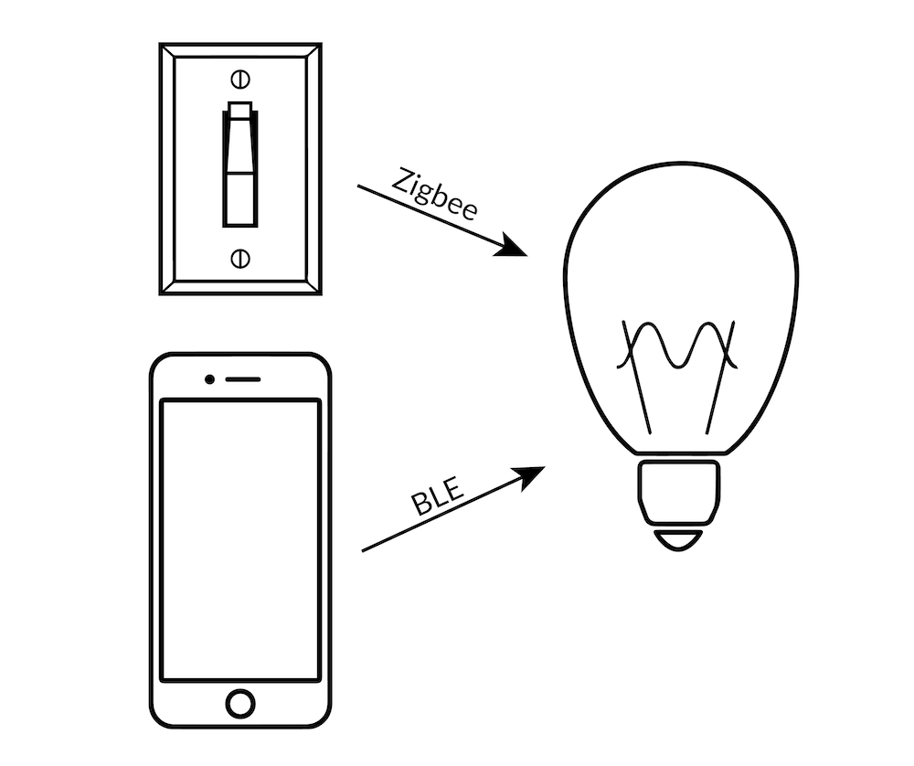
Developing multi-protocol hubs can be a challenge unless your team, like ours, has done it already. We have worked on multiple hubs including all the common standards such as Thread, Wi-Fi, Zigbee, Z-Wave and Bluetooth.
Matter-Enabled Devices
Matter has the promise of simplifying the commissioning and operation of connected devices for consumers. Realizing the dream requires a team that understands the security, how to commission over Thread, Wi-Fi, etc., and that can successfully transition from legacy standards.
Battery-Powered Wi-Fi Devices
Silicon Labs low-power Wi-Fi chips are a game changer for battery-powered devices — using less than a third of the power of their competition. Realizing all the potential power savings, while ensuring your product is quick to respond, can be a design challenge. Our engineers are used to power challenges and are experts in verifying that low-power states are maintained in real-world circumstances.
Wi-SUN Products
Need the range of LoRa but prefer to avoid the vendor lock-in that comes with a proprietary solution? Wi-SUN (Smart Ubiquitous Networks) is perfect for large-scale outdoor IoT wireless communication networks, and we can help.
Watch a video testimonial about FPT Software/Cardinal Peak’s Relationship with Silicon Labs
“Right now, the team at Hanoi is the biggest partner we have offshore… the skills, the trust, what we have with them is brilliant.” – Shoaib Javed, Director of Software Engineering, Silicon Labs
Details About Our SiLabs Design Center
Our dedicated development center supports Silicon Labs solutions, as well as more than 30 customers a year. With more than 100 employees across 11 separate teams, we provide:
- Developer services
- Sample application development
- Testing services
- End customer support
- Product development and maintenance
Across a range of SiLabs products & technologies including:
- Zigbee and Bluetooth Mesh
- Silicon Labs Xpress solutions
- Simplicity Studio
- Custom Part Manufacturing Service (CPMS)
How Our SiLabs Design Center Can Support You
With deep experience in Silicon Labs’ technologies, the design center is fast and efficient in developing your SiLabs-based products. The extensive testing network ensures that your connected products will have the highest reliability and compatibility.
With a managed offshore model, we provide onshore project managers and architects for streamlined communication working with offshore development engineers and testers. Together, they bring the benefits of a blended onshore/offshore rate. In addition, our global scale means we have personnel ready to start on your project today, getting you to market faster.
Specialized Silicon Labs Engineering Capabilities


Silicon Labs Product Development Blogs
Working With the Silicon Labs Zigbee/BLE Multiprotocol Development Kit

Amazon Sidewalk Expert On Silicon Labs’ Works With Panel
IoT Lighting with Multiprotocol Connectivity
Silicon Labs Development Services FAQs
What is a Silicon Labs Design Partner?
A Silicon Labs Design Partner is an engineering firm with verified expertise in the Silicon Labs hardware and software ecosystem. Engaging a design partner accelerates time-to-market by leveraging specialized knowledge of proprietary technologies—such as the BG24/MG24 SoCs, Simplicity Studio, and Secure Vault—ensuring that IoT products are architected correctly for power, range, and security from day one.
What is the Silicon Labs Custom Part Manufacturing Service (CPMS)?
CPMS (Custom Part Manufacturing Service) is a secure provisioning solution that allows developers to program security credentials—such as secure boot keys, certificates, and encrypted embedded software—directly at the Silicon Labs factory. This “black box” approach protects intellectual property (IP) from theft during manufacturing because sensitive keys never touch the contract manufacturer’s factory floor.
What services are typically provided by a Silicon Labs ODC?
A Silicon Labs Offshore Development Center (ODC) provides scalable, specialized engineering services focused exclusively on the Silicon Labs portfolio. Core services include custom hardware design (schematic and layout), embedded software development for mesh networking (Matter, Zigbee, Thread), automated QA testing, and long-term sustaining engineering for legacy product fleets.
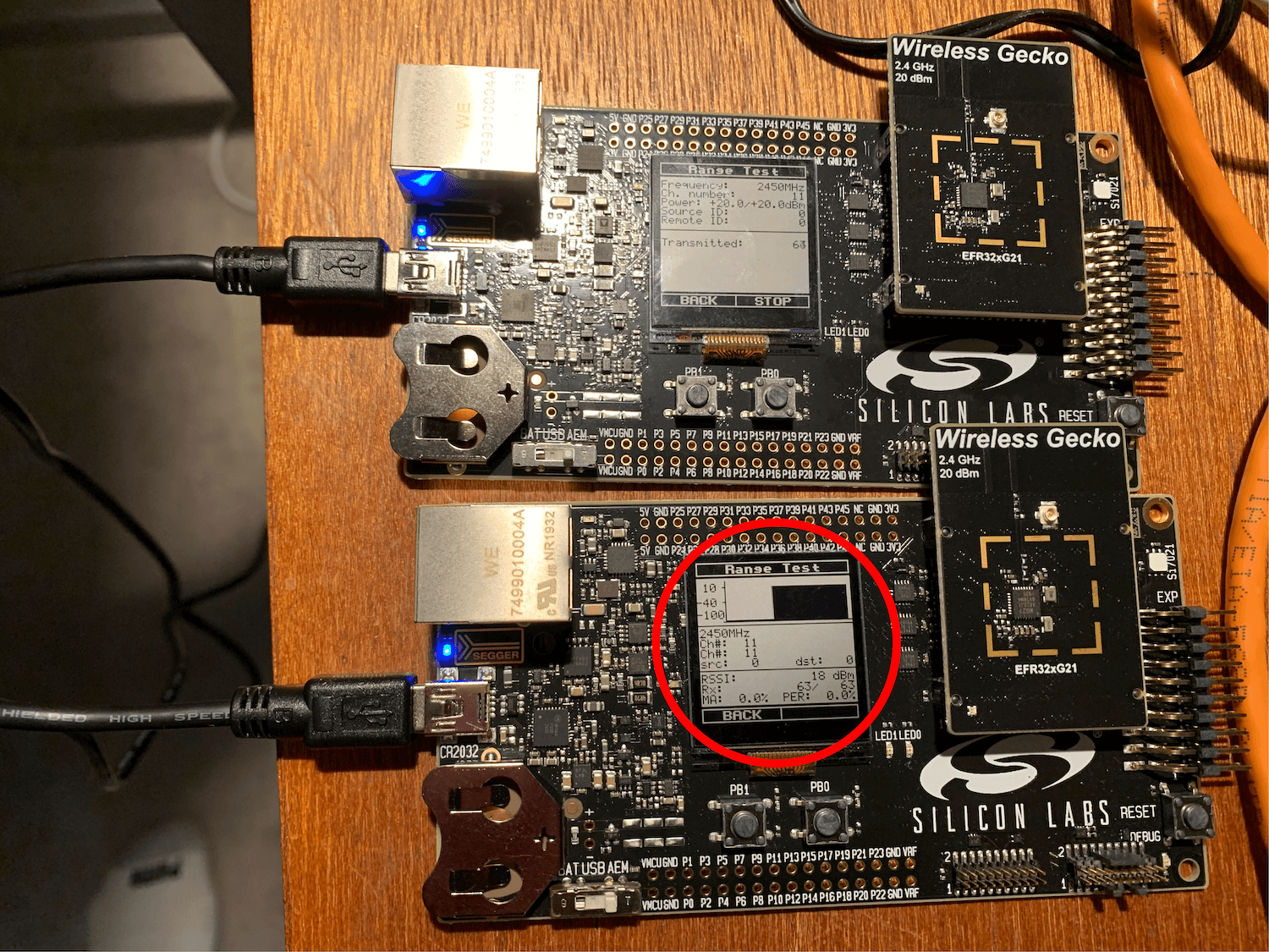
Why is automated mesh network testing important for IoT?
Automated mesh network testing is critical because wireless protocols like Matter and Zigbee behave differently at scale than they do on a workbench. A large-scale test bed (100+ nodes) simulates real-world congestion, identifying critical failures—such as packet collisions, latency spikes, and provisioning errors—that only emerge when hundreds of devices share the same network.