Writing software on an embedded device can be difficult for any number of reasons, but smart design choices up front can help mitigate some of the pain down the road. There are entire books and college courses devoted to this topic. However, I think the following three items are a good place to start.
Contents
Layered Architecture
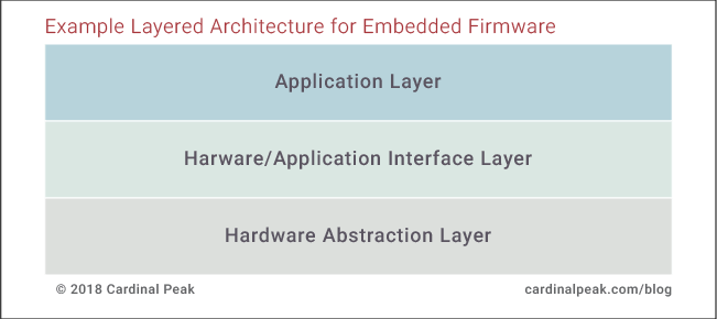
Start with a layered architecture which simply means slice the design into horizontal layers. The scope is often to communicate between hardware (sensors, buttons, cables, etc) and a user interface (LCD screen, LEDs, app, etc). In that generic case, we can split the design into three layers.

The application layer handles all of the business logic surrounding what the thing is actually supposed to do, i.e., set a timer, check the temperature, turn on a fan, unlock the door, and so on. It determines what actions need to be taken based on various inputs. Many of these inputs come directly from the hardware abstraction layer or HAL. This layer interfaces directly to the hardware elements, handles all of the specifics about how to talk to each piece of hardware, and receives the notifications that are sent directly from the hardware itself. The hardware/application interface layer sits between the two. It translates the hardware events, actions, and commands into application speak and vice versa.
Implicit in this design is the firm restriction that each layer only talks to adjoining layers, so the application layer doesn’t talk to the hardware or even the hardware abstraction layer. Instead, it tells the hardware application interface layer what needs to be done, then the interface layer translates that into hardware speak, and finally, the HAL communicates with the hardware.
Separating the design into distinct layers allows for easy parallel development if desired. The clean separation allows for defining interfaces that can eventually be tested (more on this later). It also makes problems much easier to isolate and debug.
Modular Implementation
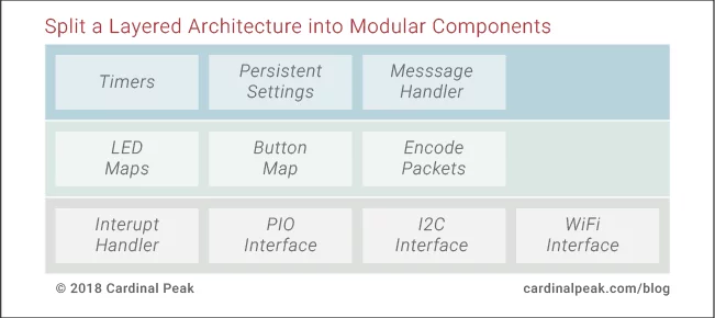
Once the layers have been identified, move towards slicing each layer into smaller, modular components. Each component should have one purpose or function, and it should own that. Here’s an example of our layered architecture split into modules.

This separation has a number of benefits. Before beginning to implement, the code is easy to understand conceptually and therefore easier to write and read. It also attempts to avoid intermixing or coupling logic unnecessarily which can lead to massive headaches while trying to maintain the code later on.
Finally, it makes the entire design more flexible to change. If a new hardware part is required, the interface to that part can easily be swapped out with minimal modifications to other areas of the code. Similarly, code can be reused on future projects or reused from previous projects to help cut down on re-writing the same code over and over.
Check out this blog about embedded software engineering services for answers to common FAQs.
Plan for Test
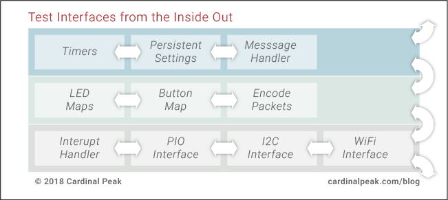
We all know the value of testing, but it can be difficult to maintain the personal, team, and management discipline to add in tests especially when the schedule seems to be slipping. However, the two guidelines above make test design easier. Test planning is almost built into the design itself if you work from the inside out. Test each module by itself. Then test the interactions between modules. Once each layer looks good on its own, test the interfaces between the layers themselves, and finally test the entire system end to end. It looks a little something like this:

It can be tempting to skip this step, but remember that your code will get tested eventually if not by you then by your customers.
Start with a layered architecture, develop modular code, and test along the way. These tips do not guarantee success, but they provide a solid foundation on which to build embedded firmware.
If your team requires embedded software engineering services or other assistance to bring your embedded system to life — connect with our engineering experts today!
